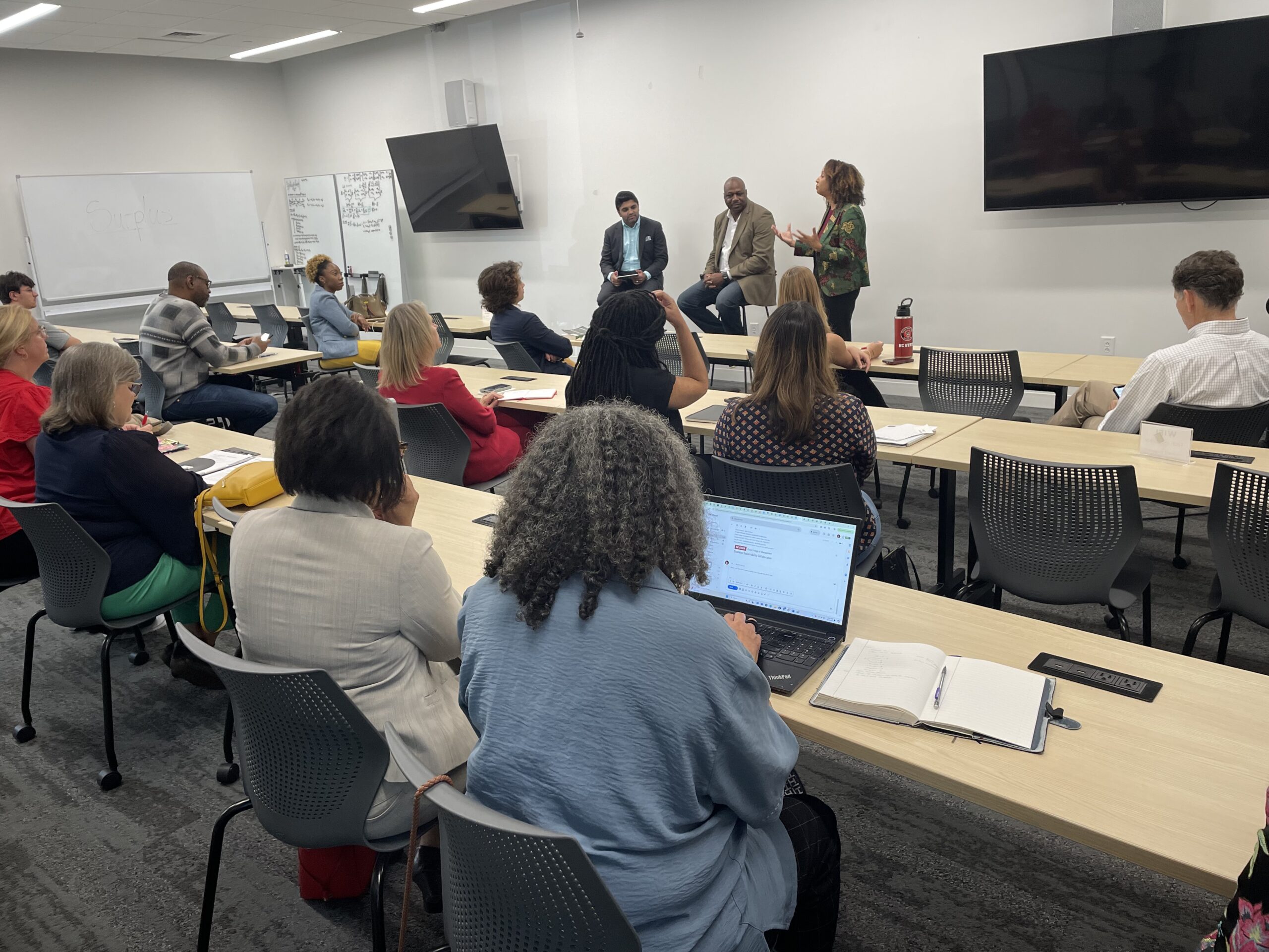
BEHIND THE SCENES OF NC STATE’S COLLABORATION WITH THE DEPARTMENT OF ENERGY
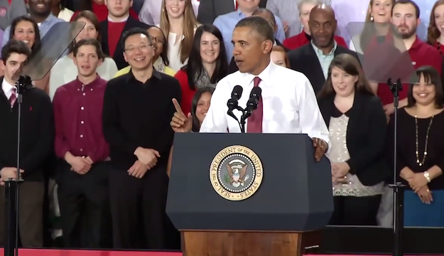
When President Barack Obama spoke at NC State University on January 15th, 2014, he was announcing a very important initiative with a somewhat unwieldy name. The Next Generation Power Electronics Manufacturing Innovation Institute is a collaboration between the Department of Energy, NC State University and whole host of other private and public sector actors with a singular mission: advancing the development, manufacturing and commercialization of Wide Band Gap (WBG) semiconductors.
We caught up with Dennis Kekas, the Acting Executive Director of the Institute, to learn more.
Can you explain a little more about the significance of WBG semiconductors?
We use silicon semiconductors in just about everything that involves electronics these days – smartphones, computers, TVs. But there are other classes of semiconductors too – most notably gallium nitride and silicon carbide wide band gap semiconductors – which offer some distinct advantages over silicon. They are higher performance, operate at higher temperatures, they handle higher voltages, and they can be significantly smaller than the semiconductors we typically use today.
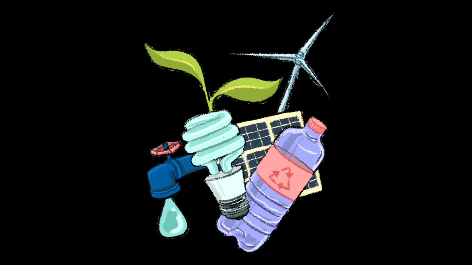
We’re already using WBG semiconductors in many applications, including LED lighting and the power amplifier inside your cell phone. But there’s growing demand for WBGs in a much broader range of applications, including electric vehicle charging, grid integration of renewables, driving energy efficient data centers, and more efficient, more compact power supplies for consumer electronics. Some of these applications will result in significant reductions in energy losses, others will be smaller gains – but taken together they represent savings of a significant slice of our energy consumption as a nation.
What role will the Institute play in bringing these innovations to market?
When I first started working at IBM, I worked on gigantic mainframe computers that took up whole rooms. Those computers had the same computing power as the phone I’m talking on today. And that’s happened because of rapid integration and reduction in the cost of silicon semiconductors.
We want to do the same thing for WBG semiconductors.
If you compare the market for WBG semiconductors to silicon, they just don’t yet have the economies of scale to compete for many of the applications where they would bring advantages. The Institute is designed to help bridge that gap, creating a network of players working together along the whole value chain – from the researchers and designers through manufacturers to the end customer. We’re going to be acting as the hub in that network — researching new applications and configurations, and then enabling collaboration that turns it into marketable solutions. We’ve got 5 universities and 18 industry partners involved, ranging from small and medium-sized enterprizes to international giants like ABB and Toshiba.
As these partnerships create new manufacturing methods and better applications, they’ll increase demand, and increased demand means more supply – soon you have the same kinds of economies of scale which have driven down the costs of computing in recent decades.
Many in the Triangle and the Research Triangle Park have already been positioning the region as a hub for green growth and clean technology. What will this new Institute mean for the region?
Much of our manufacturing as a nation has been lost to overseas competition based on cheap labor. Like the Digital Manufacturing and Design Innovation Institute and the Lightweight and Modern Metals Innovation Institute announced by the White House recently, the idea behind this initiative is also to help American manufacturing compete in the global economy – but to do so in areas of the economy where we are well placed to compete. That means strategically targeting high tech manufacturing industries that require an educated workforce.
The model behind the Institute is also a little different than previous grantmaking efforts to support industry. It used to be that government and academia would start with research into new ideas or technologies, then they’d they’d hand off to the private sector for commercialization of those ideas via reports, algorithms, prototypes etc.
That might have worked 30 years ago, but these days you have to run a little faster.
With the Institute, we’re taking technologies that are already proven, we’re building off a history of existing research, much of it here at NC State, and we’re creating a partnership of private and public sector players who can scale it up, commercialize it, and regain competitiveness for American manufacturing in the process.
What does the timeline look like for the development of the Next Generation Power Electronics National Manufacturing Innovation Institute?
We’re currently in the process of getting set up. That means drafting membership agreements, locating space, hiring staff, and we are working with the DOE to construct a cooperative research agreement. The intent is to have that done June 1st, and we’ll be ready to go and funding will start.
- Categories: